Currently, there are several technologies available in the industry for applying a solder mixture on a pad of a wafer. This technique is called a wafer bumping process. Wafer embossing using screen printing is popular as a cost-saving mass production solution. However, with the increase in the number of I/Os and the ever-decreasing spacing, the method of printing solder paste on solder joints using screen boards has become more challenging, and the matching process design requirements have also been greatly improved. Process steps Process parameters affecting wafer bump yield Copper Free Mirror,Copper Free Mirror For Shower,Copper Free Mirror Lens,Clear Copper Free Mirror Fog Dongguan Huahui Glass Manufacturing Co.,Ltd , https://www.antiquemirrorsupplier.com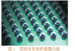
Why screen printing?
The industry's three most famous wafer bumping methods - screen printing, evaporation and sputtering or electroplating - each have their own advantages and disadvantages (Table 1). The choice of method, in addition to the need to consider the company's process roadmap, more importantly, there are many parameters to consider, including bump pitch, bump height, wafer base material, wafer thickness, wafer size, bump uniformity , as well as raised material.
Equipment and Materials <br> Wafer bump printing methods are designed to be compatible with the tools of a standard surface mount assembly line, so no additional investment is required when upgrading or retrofitting existing large equipment.
However, screen printing machines should be equipped with sophisticated optical devices. The alignment system should be able to identify non-standard reference points on the processed wafer, including pad corners, special marks, marks, or other metallized features that contrast sharply with the background cover.
In the printing process, in order to ensure the safe handling of precision wafers, rigid pallets are needed to support the wafers.
Wafer bumps typically use water-soluble solder paste. The bumps must be clean and easy to be fluxed during subsequent flip-chip assembly to achieve stable wetting and consistent adhesion; in addition, to minimize any buildup on the bumps or between the bumps. The material can make the bottom flip chip filling process more reliable after assembly. So far, there is no commercially available non-clean paste material that can achieve residue-free solder joints.
Wafer raised printing
The process is similar to printing on FR-4 substrates. The wafer is first placed on a tray and conveyed by a conveyor belt to a screen printer. Then, for the squeegee printing method, the solder paste is first agitated for 30 to 60 seconds to prepare for the filling, which is to uniformly apply the flux and Solder powder and the important step of diluting the solder paste to a suitable consistency (using a cartridge-type closed print head system with automatic infusion and stir-weld functions, this step can be omitted); then, applying the solder paste to the screen Afterwards, the printer's video system finds all reference points, cleans the solder paste across the surface of the screen, and injects it into all the openings; finally, the trays and wafers are conveyed from the printer.
Positioning check
Using a microscope for solder paste deposition and positioning verification, the solder paste deposits should be properly aligned to cover all solder pads, which is a key element in ensuring a robust reflow soldering process. For high-density fine-pitch configurations, achieving perfect alignment is a challenging task, and manual offset alignment is sometimes programmed.
Reflow
Once the alignment of the solder paste is verified, the printed wafer can be reflowed in a forced convection oven.
Cleaning and drying
In the cleaning process, the wafer is rinsed with mild deionized water to remove the water-soluble flux. Then dry the wafer with clean forced convection air or nitrogen. Finally, it is recommended that the wafer be dehydrated and baked at 125°C for two hours to remove any moisture that the wafer may absorb during the cleaning process.
Clean stencil
The cleanliness of the screen is also crucial. Even after a single printing stroke, the inner wall of the screen opening will accumulate a lot of solder paste residue. It will soon dry out and smear the subsequent printing stroke.
Many variables can seriously affect the quality or yield of wafers using such bumping methods. Known good die (KGD) values ​​are commonly used to represent wafer bumping process performance. The most important factors to consider when successfully implementing a wafer printing process include: solder paste, printing environment (environment and humidity), printer settings, reflow conditions, and cleaning options.
Solder paste
An important characteristic of solder paste is the particle size and distribution, which depends primarily on the amount of solder paste deposited, as well as the size of the openings in the mesh. It is generally believed that the particle size of the solder paste should be such that the diameter of at least three of the largest solder balls conforms to the width of the smallest opening on the screen. This is known as the "three ball law." The distribution and density of the solder particles directly affect the rheological properties of the solder paste and also affect its performance on the screen printing machine.
It is best to use the finest solder powder for wafer screen printing; it is reported that the Sn63/Pb37 V solder paste has a 90% metal content distribution and can be effectively used for 8 mil pitch bump processing. Raised height reaches 5 mils.
Solder paste for wafer printing has shorter exposure time and effective life cycle than the standard value of SMT solder paste. In order to maximize the life cycle of the solder paste, the solder paste should be removed from the screen as long as the press is idle. An important advantage of using closed transfer printing is that the solder paste is always closed and isolated from the surrounding environment.
Designing an Ideal Wafer Raised Screen Printing Process (I)